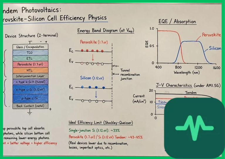
Bandgap Engineering and Spectral Photon Harvesting
The foundational physical principle enabling tandem solar cell efficiency gains is complementary bandgap tuning. The solar spectrum spans a broad photon energy range from ultraviolet to infrared. A single semiconductor material possesses a fixed bandgap ( ); photons with energy below
 cannot excite electrons across the valence band to the conduction band, whereas photons with energy significantly exceeding
 waste surplus kinetic energy as lattice heat.
Perovskite-silicon tandem devices resolve this thermodynamic loss by pairing semiconductors with mismatched optical bandgaps:
- Perovskite Top Cell: Formulated with an engineered wide bandgap ranging from
 to
 , the metal halide perovskite top layer—typically comprising mixed-cation lead halides such as formamidinium cesium lead trihalide (
 )—absorbs high-energy visible photons (wavelengths under
 to
 ).
- Silicon Bottom Cell: Featuring an optimized narrow bandgap of approximately
 , the underlying crystalline silicon substrate transmits high-energy visible light harmlessly through the transparent top contact while absorbing transmitted near-infrared photons ranging from
 to
 .
This dual-junction configuration divides the solar spectrum into distinct thermodynamic segments, drastically reducing thermalization losses and elevating the theoretical multi-junction efficiency ceiling above 42%.
Monolithic Versus Four-Terminal Tandem Architectures
Engineering tandem photovoltaic modules requires selecting between two primary electrical connection topologies: monolithic two-terminal (2T) designs and mechanically stacked four-terminal (4T) configurations.
In a monolithic two-terminal tandem cell, the perovskite top subcell and the silicon bottom subcell are grown sequentially on a single substrate, interconnected in series via an ultrathin recombination layer (such as indium tin oxide [ ) or heavily doped zinc oxide (
 ). Because both subcells are connected in series, the total operating current of the tandem device is strictly constrained by the lower current of the two subcells. Consequently, manufacturing monolithic 2T tandems demands rigorous optical and electrical current matching (
 ) under operational AM1.5G solar illumination. Any spectral shift or optical parasitic absorption in the top layers creates current mismatching, leading to severe fill factor (
 ) losses and diminished power output.
Conversely, four-terminal (4T) tandem configurations isolate the top and bottom subcells electrically, mounting them as independent devices with separate wiring circuits. This decoupling eliminates current-matching constraints, simplifying fabrication and allowing each subcell to operate at its individual maximum power point (MPP). However, 4T architectures require complex dual-inverter balance-of-system wiring and introduce front-surface reflection and parasitic optical absorption losses from intermediate transparent conductive glass slides, reducing overall module-level power density compared to optimized monolithic 2T designs.
Technical Data Specifications of Perovskite-Silicon Tandem Parameters
| Tandem Photovoltaic Parameter | Engineering Specification Standard |
|---|---|
Perovskite Top Cell Bandgap ( ) |  to  wide-bandgap formulation |
Silicon Bottom Cell Bandgap ( ) |  crystalline silicon baseline |
| Theoretical Efficiency Limit (2-Junction) | ~42.5% Shockley-Queisser multi-junction limit |
| Certified Laboratory Efficiency (2T) | 33.2% to 34.6% active area conversion yield |
| Monolithic Current Matching Requirement |  series current equalization |
| Operational Temperature Coefficient | 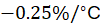 to 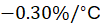 power loss metric |
| Perovskite Layer Thickness Range |  to  (  to  ) |
Interfacial Charge Extraction and Recombination Mechanics
Achieving high open-circuit voltages ( ) and fill factors in perovskite-silicon tandems requires optimizing charge transport layers and minimizing non-radiative recombination losses at semiconductor interfaces. When photogenerated electrons and holes separate within the perovskite crystal lattice, they must traverse selective contact layers before reaching external electrodes.
Engineers deploy specialized organic or inorganic charge transport materials:
- Electron Transport Layers (ETL): Materials such as fullerene derivatives (
 ) or tin oxide (
 ) nanoparticles deposited via atomic layer deposition (ALD) extract electrons efficiently while blocking hole back-flow.
- Hole Transport Layers (HTL): Self-assembled monolayers (SAMs)—such as carbazole-based molecules like Me-4PACz—form uniform molecular monolayers on textured silicon pyramids, establishing low-resistance ohmic contacts and eliminating parasitic optical absorption at the perovskite-silicon interface.
Defect passivation strategies using organic halide salts (such as phenethylammonium iodide) suppress trap-assisted recombination at grain boundaries and surface interfaces, boosting voltage outputs and pushing tandem device  metrics beyond
 to
 .
Thermal Stability Degradation and Moisture Resistance
Despite exceptional laboratory power conversion efficiencies, commercializing perovskite-silicon tandem modules requires resolving severe material stability challenges. Metal halide perovskite crystal structures are inherently vulnerable to environmental degradation induced by moisture, ultraviolet (UV) radiation, oxygen ingress, and elevated operating temperatures.
When exposed to ambient moisture or operational temperatures exceeding  to
 (
 to
 ), the perovskite active layer decomposes back into its constituent lead halides and organic salts, triggering phase segregation and irreversible photocurrent loss. Industrial module manufacturers mitigate these degradation pathways by implementing edge-seal barrier polymers, atomic-layer-deposited impermeable metal-oxide encapsulation layers, and compositional engineering (substituting volatile organic methylammonium cations with photochemically stable cesium and rubidium dopants). Accelerated thermal stress testing confirms that passivated encapsulation architectures achieve operational lifetimes exceeding 25 years under standard IEC 61215 stress protocols.
The Final Take
Mastering perovskite-silicon tandem solar cell efficiency physics redefines photovoltaic engineering by breaking through single-junction thermodynamic limits. Citing IEA photovoltaic roadmaps and semiconductor physics literature, dual-junction bandgap engineering captures a broader segment of the solar spectrum, elevating laboratory conversion efficiencies beyond 34%. By optimizing monolithic current matching, interfacial charge transport, and encapsulation stability, perovskite-silicon tandems establish an essential technical foundation for high-efficiency global solar power generation.



Comments (0)
Login to leave a comment.
No comments yet. Be the first to share your thoughts!