

Bandgap Energy Optimization and Multi-Junction Physics
The foundational physical limitation governing single-junction solar cells is spectral mismatch. Photons with energy below the semiconductor bandgap ( ) pass through the material without being absorbed, while photons possessing energy significantly exceeding the bandgap waste excess energy as heat through thermalization of hot charge carriers.
Perovskite-silicon tandem solar cells overcome this thermodynamic restriction by splitting the solar spectrum across two complementary active absorber layers with mismatched bandgap energies:
- Perovskite Top Cell: Engineered with a wide bandgap ranging from
 to
 , the metal halide perovskite layer absorbs high-energy ultraviolet and visible photons (wavelengths below
 ), converting them efficiently while minimizing thermalization losses.
- Silicon Bottom Cell: Operating with a narrow bandgap of
 , the underlying crystalline silicon wafer transmits high-energy photons but absorbs lower-energy near-infrared photons (wavelengths spanning
 to
 ) that pass unabsorbed through the upper perovskite layer.
The theoretical tandem efficiency ( ) is governed by optimizing the cumulative open-circuit voltage (
 ) of both sub-cells while maintaining matched short-circuit current densities (
 ), formulated mathematically in monolithic two-terminal configurations as:

Achieving current matching prevents electrical bottlenecks where one sub-cell limits the total current throughput of the series-connected tandem stack.
Optical Absorption Coefficients and Spectrum Splitting
Metal halide perovskites—represented by the chemical formula  (where A is cesium, formamidinium, or methylammonium; B is lead or tin; and X is iodine, bromine, or chlorine)—exhibit exceptionally high optical absorption coefficients (
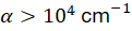 ) across the visible spectrum. This steep absorption coefficient enables ultra-thin perovskite absorber layers (
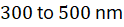 [
 ]) to absorb incoming high-energy radiation completely.
Unabsorbed near-infrared photons pass downward through the transparent rear electrode and intermediate recombination layer into the silicon bottom cell. Advanced optical management utilizes textured silicon wafer surfaces and antireflective dielectric coatings ( or
 ) to minimize parasitic reflection losses and trap light within both sub-cells, maximizing total photon conversion efficiency.
Technical Data Specifications of Tandem Solar Cells
| Tandem Solar Cell Parameter | Engineering & Material Specification Standard |
|---|---|
Perovskite Top Cell Bandgap ( ) |  to  spectral optimization |
Silicon Bottom Cell Bandgap ( ) |  standard crystalline silicon |
| Monolithic Tandem Efficiency Record | 33% to 35% certified laboratory conversion metric |
| Perovskite Absorber Layer Thickness |  to  (  ) |
Optical Absorption Coefficient ( ) | 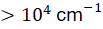 across visible spectrum |
Temperature Coefficient ( ) | 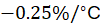 to 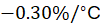 improved thermal stability |
| Operational Operating Temperature |  to  (  to  ) nominal |
Recombination Losses and Interlayer Contact Engineering
Monolithic two-terminal perovskite-silicon tandem cells require an engineered interlayer recombination junction (or tunnel junction) that electrically connects the bottom of the perovskite top cell to the top of the silicon bottom cell without introducing optical parasitic absorption or high electrical resistance.
This interlayer typically incorporates ultra-thin transparent conductive oxide (TCO) films—such as indium tin oxide (ITO) or doped zinc oxide ( )—combined with charge-selective transport layers. Hole transport layers (HTL) like Spiro-MeOTAD or poly(triarylamine) (PTAA) extract photogenerated holes from the perovskite valence band, while electron transport layers (ETL) like tin dioxide (
 ) extract electrons.
If interfacial defect density is high, charge carriers undergo non-radiative recombination at the interlayer boundary, reducing the fill factor (FF) and open-circuit voltage. Deploying self-assembled monolayers (SAMs) at the buried interface passivates surface dangling bonds, reducing interfacial recombination velocity and elevating tandem fill factors above 82%.
Thermal Stability Degradation and Moisture Sensitivity
A major technical barrier commercializing perovskite-silicon tandem solar cells is thermal stability degradation and environmental vulnerability. Unlike stable crystalline silicon modules possessing multi-decade operational lifespans, lead halide perovskite crystals are chemically fragile when exposed to ambient moisture, ultraviolet (UV) irradiation, and elevated operational temperatures.
Under high operating temperatures ( to
 [
 to
 ]) experienced outdoors, mixed-cation perovskite compositions undergo phase segregation, where iodide-rich and bromide-rich domains separate spontaneously. This phase segregation alters local bandgap energies and degrades open-circuit voltage. Furthermore, moisture ingress triggers crystal decomposition of the
 lattice back into lead iodide (
 ) and organic precursors.
To mitigate degradation, manufacturers apply robust edge-sealant encapsulation and atomic layer deposition (ALD) barrier layers of aluminum oxide ( ), sealing the module against atmospheric humidity and stabilizing commercial outdoor performance.


Comments (0)
Login to leave a comment.
No comments yet. Be the first to share your thoughts!