
Photovoltaic Bandgap Engineering and Spectral Utilization
Single-junction solar cells are bound by fundamental thermodynamic loss mechanisms. Photons with energy below the semiconductor bandgap ( ) pass through the material entirely unabsorbed, while photons with energy exceeding the bandgap waste excess energy as thermal lattice vibrations, known as thermalization. For a single-junction crystalline silicon cell with an optimum bandgap of
 , the theoretical maximum efficiency limit is approximately 33% under standard AM1.5G solar illumination.
Tandem architectures resolve this restriction by dividing the solar spectrum across two or more sub-cells. They include:
- Top Cell Optimization: The wide-bandgap perovskite top cell absorbs high-energy ultraviolet and visible photons (wavelengths below
 ), typically featuring a bandgap engineered between
 and
 .
- Bottom Cell Optimization: Lower-energy near-infrared photons pass transparently through the top cell to be absorbed by the underlying low-bandgap silicon (
 ) or tin-lead perovskite (
 ) bottom cell.
By matching dual absorption thresholds to distinct photon energy bands, tandem configurations elevate theoretical single-side conversion limits past 43% under one-sun illumination.
Crystal Structure and Halide Composition Tuning
The active light-absorbing material in the top cell consists of metal halide perovskites conforming to the general chemical formula  , where
 represents a monovalent cation (such as formamidinium
 , cesium
 , or methylammonium
 ),
 represents a divalent metal cation (lead
 or tin
 ), and
 represents a halide anion (iodine
 , bromine
 , or chlorine
 ).
Precise bandgap tuning is achieved through halide substitution ratios. Increasing the molar concentration of bromine relative to iodine widens the crystal lattice bandgap toward  , optimizing photon absorption for the top tandem sub-cell. However, high-bromine compositions (
 molar ratio) subjected to illumination suffer from halide segregation—a thermodynamic phenomenon where mixed halides phase-separate into iodine-rich and bromine-rich domains. This phase separation creates localized low-bandgap traps, inducing voltage drops and steady-state efficiency degradation. Researchers suppress halide segregation by incorporating rubidium cations and passivating grain boundaries with alkylammonium halide additives.
Monolithic Two-Terminal (2T) vs. Four-Terminal (4T) Architectures
Integrating sub-cells into a functional module relies on two distinct electrical configurations, each presenting unique engineering trade-offs:
- Two-Terminal (2T) Monolithic Tandems: The perovskite top cell is processed directly on top of the silicon bottom cell using solution-processed or vapor-deposited layers. Both sub-cells are connected in series through an intermediate recombination layer. Current matching is mandatory; the photocurrent generated by the top cell must exactly equal the photocurrent of the bottom cell (
 ) to prevent current bottlenecks and severe fill factor losses.
- Four-Terminal (4T) Mechanically Stacked Tandems: The top and bottom sub-cells operate independently on separate electrical circuits, separated by an air gap or optical coupling medium. This configuration eliminates current-matching constraints, simplifying manufacturing tolerances. However, 4T systems require four distinct busbar connections, independent maximum power point tracking (MPPT) inverters, and transparent conductive oxide (TCO) layers that incur parasitic optical absorption losses.
Recombination Layer Physics and Interfacial Charge Transfer
In monolithic 2T tandem devices, the intermediate interconnecting layer—often termed the recombination layer or tunnel junction—must facilitate seamless electron-hole recombination between the n-type contact of the top cell and the p-type contact of the bottom cell without introducing parasitic optical reflection or voltage losses.
Advanced devices utilize reactive-plasma-deposited (RPD) indium oxide co-doped with cerium and hydrogen (ICO:H) combined with self-assembled monolayers (SAMs) such as carbazole-based molecules (e.g., MeO-PACz). This interface engineering promotes uniform wetting, ensures robust adhesion during high-throughput slot-die coating or vacuum evaporation, and establishes low-resistance ohmic contact. Minimizing series resistance at this internal junction is essential for maintaining a high fill factor ( ) exceeding 82% in laboratory-scale cells.
Degradation Kinetics and Long-Term Thermal Stability
Despite exceptional laboratory power conversion efficiencies, commercial deployment requires meeting stringent outdoor operational lifetimes of 25 to 30 years, governed by international testing protocols such as IEC 61215. Perovskite materials exhibit intrinsic vulnerability to environmental stressors, including moisture ingress, ultraviolet (UV) irradiation, oxygen exposure, and elevated temperatures exceeding  (
 ).
Moisture catalyzes the hydrolysis of formamidinium lead triiodide ( ), decomposing the crystal lattice into yellow lead iodide (
 ) and volatile organic byproducts. Furthermore, thermal stress triggers ion migration within the perovskite bulk, causing metal electrode corrosion and delamination at charge-transport interfaces. Modern encapsulation strategies utilize cross-linked epoxy polymers and polyisobutylene edge seals combined with atomic layer deposition (ALD) aluminum oxide (
 ) barrier films. These protective layers prevent water vapor transmission rates (WVTR) from exceeding
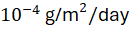 , successfully passing 1,000 hours of damp-heat testing (
 [
 ] and 85% relative humidity) with minimal power degradation.
Empirical Performance Metrics and Commercial Scalability
Empirical trends compiled by the IEA and academic research consortia confirm that perovskite-silicon tandem modules have rapidly transitioned from academic curiosities into pilot-scale industrial production. While small-area laboratory cells achieve certified efficiencies above 35%, scaling active surface areas to full commercial module formats (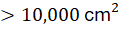 or
 ) introduces non-uniform layer thicknesses, increased series resistance, and edge-defect density.
Industrial manufacturing lines address the efficiency-area trade-off by employing advanced meniscus slot-die coating and co-evaporation techniques that maintain compositional uniformity across large substrates. Techno-economic assessments project that commercial tandem modules achieving 28% to 32% operational efficiency will reduce levelized costs of electricity (LCOE) below utility-scale monofacial silicon thresholds, accelerating global decarbonization trajectories.



Comments (0)
Login to leave a comment.
No comments yet. Be the first to share your thoughts!